Digital Controller of a Single-Inductor, Dual-Output Switch Converter
本文于1417天之前发表,文中内容可能已经过时。如有疑问,请在评论区留言。
A digital controller for single-inductor dual-output switching converter with low cross regulation
Supervisor of this research is Lecture .
Circuit Structure
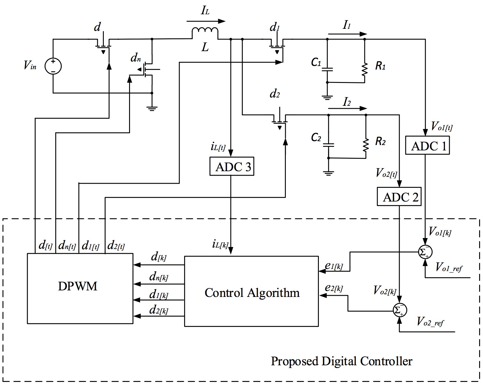
The whole structure of this research uses the digital controller’s SIDO buck converter. A/D converter(ADC) was used to sample the output voltage and inductance current of the two output branches and several PWM driven transistors were used as switches to control the output voltage. The digital duty cycle of each switch cycle is calculated by digital control algorithm, and the final duty cycle signal of switch tube is converted by DPWM module.
Output and Steady State
The waveform of output voltage, inductance current and duty cycle signal is shown in the figure.
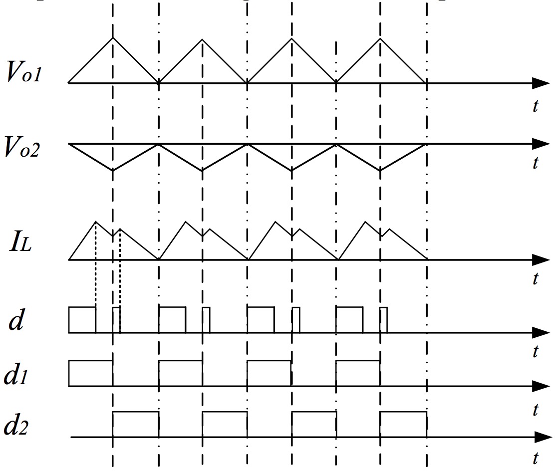
During each period, when one output branch is charged, the other output branch will be discharged. By calculating the output current and inductance current in each cycle, the relationship between each voltage output capacitor and inductance is found.
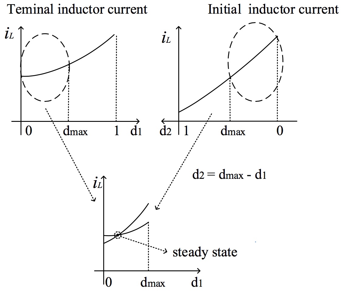
When any branch of the SIDO converter reaches steady state, the charging capacity of the output capacitor must be equal to that of the output capacitor. In order to meet the steady-state condition, the initial inductance current and duty cycle can be changed in a certain range at the beginning of each cycle. For each output branch, it has a specific initial inductance current and duty cycle range to meet the steady-state conditions. At the same time, the SIDO converter requires two output branches to reach steady state in steady state, and the terminal charging inductance current of one branch is also the initial charging inductance current of the other branch. This is the intersection of the steady-state range of the two branches, which is the steady state of the SIDO converter.
The Predictive Control Method
For SIDO converter, cross regulation is inevitable in the transient process. When the load condition of one output branch changes, the steady-state point of the SIDO converter will also change. The new and old stability points are shown in the figure.
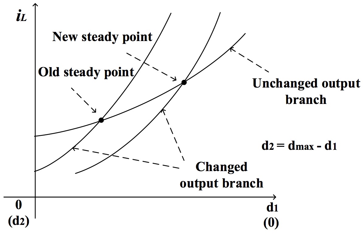
In the process of transition from the old stable point to the new one, if the relationship between the inductance current and the duty cycle of the invariant output branch is always as shown in the figure, the cross regulation of the two output branches can be effectively reduced to the minimum. In order to reduce cross regulation, a new steady state point must be determined. At the beginning of each switching cycle, the output voltage, inductance current and load current are sampled.
Simulation Verification of the SIDO Converter Resistance to External Interference
Therefore, the inductance current can be predicted. The SIDO buck switching converter with the proposed digital controller has been simulated via the Matlab/Simulink environment.
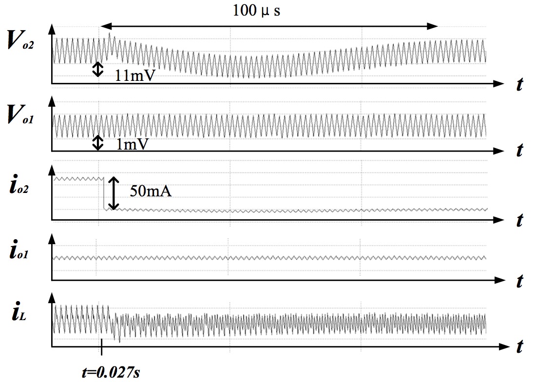
The figure shows the output voltage, output current and inductance current of the two output branches of the SIDO converter. When the output load current io2 of the second output branch changes, it is observed that the maximum voltage fluctuation of the first output branch is 11mv.
Conclusion
The pdf file of this publicationSimulation results show that the SIDO buck converter has good performance in suppressing cross regulation of output voltage.


